Project record / Deep Dive
Raspberry Pi Audio HAT with PCM5102A and Relay Input Switching
Custom Raspberry Pi audio board combining a PCM5102A I²S DAC with relay switching between DAC audio and an external stereo input.

Overview
TL;DR
A custom Raspberry Pi audio board was designed around the PCM5102A I²S DAC, with separate analog and digital 3.3 V supplies and a DPDT relay that selects between DAC audio and an external stereo input. The relay is controlled from the Pi through a 2N7002 MOSFET, while GPIO-controlled mute and DAC filter selection and two additional SMD buttons are included. The schematic has been completed and PCB placement, routing, and BOM optimization are ongoing
Key points
Features
- PCM5102A stereo I²S DAC
- Relay selection between DAC output and external stereo input
- Separate 3.3 V analog and digital LDO supplies
- GPIO-controlled DAC mute
- GPIO-controlled PCM5102A filter selection
- Two configurable SMD buttons
- Stereo 3.5 mm input and output
Entry 01
Problem
The Raspberry Pi Zero 2 W has no analog audio jack. An initial GPIO/PWM audio approach was investigated, but the target application was music playback and the project moved toward a dedicated DAC board instead. The board also needed to switch a stereo output between audio generated by the Raspberry Pi and an external stereo input. It should act as an inline solution to add Airplay to existing sound systems with limited Inputs
Entry 02
Solution
The design uses a PCM5102A to convert I²S audio from the Raspberry Pi into stereo analog audio. A G6S-2-DC5 DPDT relay switches both stereo channels together between the DAC path and an external 3.5 mm input.
The relay coil is supplied from 5 V and switched on the low side with a 2N7002 N-channel MOSFET. A 1N4148W is used as the flyback diode. The design also exposes two SMD buttons and uses Raspberry Pi GPIOs to control the PCM5102A mute and filter-selection inputs.
Entry 03
Architecture
The Raspberry Pi connects to the PCM5102A through the three I²S signals BCK, LRCK, and DIN. The I²S lines include 33 Ω series resistors.
The 5 V supply from the Raspberry Pi feeds two separate MCP1700T-3302 3.3 V LDO regulators. One supply is used for the DAC's analog supply domain and one for its digital supply domain. Local supply and charge-pump capacitors are placed around the PCM5102A.
Each DAC output passes through a 470 Ω / 2.2 nF RC network before reaching one input of the DPDT relay. The external stereo input connects to the relay's other input, and the relay common contacts feed the stereo output.
The relay-control path consists of a Raspberry Pi GPIO, a 1 kΩ gate resistor, a 2N7002, a 100 kΩ gate pulldown, a 1N4148W flyback diode, and local 100 nF supply decoupling.
GPIO5 on physical pin 29 and GPIO6 on physical pin 31 were selected for PCM5102A configuration control. XSMT and FLT each use a 100 kΩ pulldown so that the DAC starts muted and with the selected LOW-state filter setting during boot.
Entry 04
Implementation
The schematic was developed in EasyEDA Pro. The PCM5102A charge-pump network includes local capacitors for CPVDD, CAPP/CAPM, and VNEG, while AVDD and DVDD have their own local decoupling.
Space immediately around the DAC became limited with 0603 components, so the critical supply and charge-pump capacitors were moved toward 0402 packages while less placement-sensitive parts could remain 0603.
The PCB is being designed as a Raspberry Pi 40-pin-header board. Placement and routing work has included keeping the DAC output path short, positioning I²S series resistors near the Raspberry Pi side, and determining routes for additional audio breakout connections around the relay.
The BOM is also being optimized for JLCPCB assembly by reducing the number of parts taken from the Extended Parts library while retaining required components.
Entry 05
Biggest challenge
The main unresolved work is translating the completed schematic into a compact first PCB layout without compromising the audio and digital signal paths.
The area around the PCM5102A became crowded because several local capacitors need to be close to the device, leading to the decision to use smaller 0402 packages for the most placement-sensitive components.
BCK also originates from Raspberry Pi physical pin 12 in the selected I²S connection, and the current component placement makes its route approximately 4–5 cm longer than the LRCK and DIN routes. The routing has not yet been validated on fabricated hardware.
Routing L_IN and L_OUT to breakout connections created another placement constraint because a direct route would cross the DAC-output traces. Routing around or beneath the relay body was considered while keeping the relay's audio contacts and coil-control routing separated.
Entry 06
Result
The current result is a completed schematic containing the Raspberry Pi interface, PCM5102A DAC and supply circuitry, stereo relay switching, two SMD buttons, GPIO-controlled mute and filter selection, and stereo input/output connections.
PCB placement, routing, footprint optimization, and JLCPCB BOM optimization are still in progress. No fabricated PCB, audio measurement, listening result, noise measurement, distortion measurement is yet done.
Technical evidence
Project gallery


Tools and platforms
Technologies
- Raspberry Pi Zero 2 W
- PCM5102A
- EasyEDA Pro
- JLCPCB
Next reading
Related projects
Project2026
Audio Switcher HAT
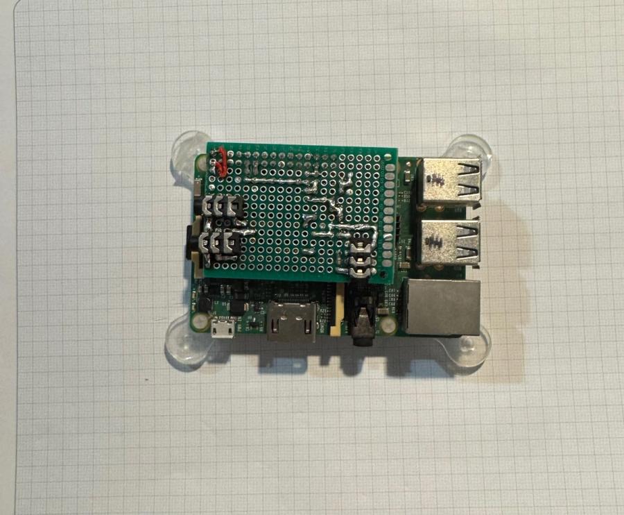
A compact, perfboard-based Raspberry Pi HAT that automatically switches stereo audio sources using a GPIO-controlled relay when an AirPlay 2 client connects.
Electronics · Embedded Systems · Automation & Control · Software · Fabrication
- Raspberry Pi 3B
- Shairport Sync
- AirPlay 2